
1–3% Efficiency Edge: N-Type vs P-Type Solar for Homeowners
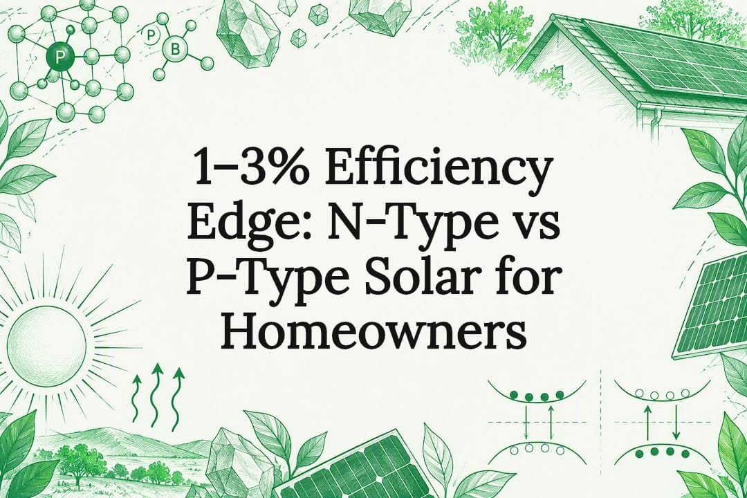
The core difference is chemical: n-type silicon is doped with phosphorus, which adds free electrons as the majority charge carrier, while p-type silicon is doped with boron, which creates “holes” that carry charge instead. For solar buyers, that single distinction cascades into real performance gaps: n-type architectures like TOPCon and HJT typically run 1 to 3% more efficient with lower degradation, while p-type PERC stays cheaper and easier to source. In 2026, most homeowners installing new residential systems are better served by n-type, unless budget is the deciding factor.
TL;DR:
- N-type solar panels typically have 2 to 3% higher efficiency and 1 to 3% lower degradation over 25 years compared to p-type PERC modules.
- The main performance advantage of n-type panels comes from longer carrier lifetimes and lower light-induced degradation, especially in the first year.
- N-type architectures like TOPCon and HJT now hold roughly 70% market share, driven by their physical benefits and reduced long-term performance loss.
- P-type panels remain cheaper and easier to manufacture, making them a viable choice for budget-conscious installations with ample roof space.
- When choosing panels, verify specific architecture and warranty details, and prioritize long-term energy yield over initial efficiency percentages.
Table of Contents
- N type vs p type comparison at a glance
- What makes n-type semiconductors different
- What makes p-type semiconductors different
- How the pn junction actually generates power
- N-type vs p-type solar panels in the real world
- Degradation risks and what to ask before you sign
- How to choose between n-type and p-type for your home
- Beyond solar: how doping reshapes the band structure
- Manufacturing challenges unique to each doping process
- Where n-type and p-type materials show up beyond your roof
- Material availability and the environmental angle
- The technology shift matters more than the marketing around it
- Get a personalised comparison before you decide
- Sources
- FAQ
N type vs p type comparison at a glance
The numbers below explain why the solar industry has swung so decisively towards n-type wafers in the past two years. Every figure is a typical industry range rather than a fixed spec, since actual performance depends on the specific cell architecture, manufacturer and installation conditions.
| Metric | N-type (TOPCon / HJT) | P-type (PERC) |
|---|---|---|
| Commercial module efficiency | 22–24.5% | 20–22% |
| First-year LID/LeTID | Very low, typically under 0.5% | 1–3% (boron-oxygen LID) |
| Annual degradation rate | 0.25–0.4% per year | 0.45–0.6% per year |
| Temperature coefficient | Around −0.29% to −0.34% per °C | Around −0.35% to −0.41% per °C |
| Bifacial gain potential | 5–15% (HJT can exceed this) | Typically 0–10%, fewer bifacial options |
| Typical cost premium | a modest cost premium over PERC (5–10% over PERC) | Baseline cost |
| Typical 25-year power retention | 87–92% | 82–87% |
These ranges reflect industry-wide comparisons of n-type and p-type cell performance, which found that n-type panels combine a meaningful efficiency edge with slower long-term decline. The market has responded accordingly: IEA PVPS data shows n-type wafer market share rose from roughly 30% to 70% between 2023 and 2024 alone, a shift that’s rarely seen this fast in any manufacturing sector.
Two things are worth separating in that table. The efficiency, degradation and temperature figures are physical properties tied to the cell architecture itself. Warranty and power-retention figures, by contrast, are manufacturer commitments, meaning two panels with identical silicon can still carry different guarantees depending on the brand’s confidence in its own production line. When comparing quotes, always ask whether the number quoted is a lab-tested range or the manufacturer’s contractual promise.
What makes n-type semiconductors different
N-type silicon starts as a pure crystal lattice, then gets doped with a pentavalent element, almost always phosphorus, occasionally arsenic. Phosphorus atoms have five outer electrons, one more than silicon needs to complete its four-bond lattice structure. That spare electron becomes mobile, free to carry charge through the material without needing a partner.
This is where the terminology “majority carrier” comes from. In n-type material, free electrons vastly outnumber the naturally occurring holes, so electrons do almost all the electrical work. The doping also shifts the material’s Fermi level, the energy threshold that determines how easily electrons flow, closer to the conduction band. In practical terms, that shift is what gives n-type material its distinct electrical behaviour compared with undoped or p-type silicon.
Why does any of this matter to someone buying a solar panel? Because carrier lifetime, how long an electron or hole survives before it recombines and is lost as heat rather than usable current, differs sharply between the two materials. Extrinsic doping fundamentally governs how many majority and minority carriers a semiconductor produces, and n-type silicon generally supports longer carrier lifetimes than boron-doped p-type material. Longer carrier lifetime means fewer electrons are lost to recombination before they reach the external circuit, which directly lifts the cell’s open-circuit voltage and, in turn, its overall efficiency.
That physical advantage is exactly why manufacturers built entire cell architectures around n-type wafers:
- TOPCon (Tunnel Oxide Passivated Contact): adds an ultra-thin oxide layer plus a doped polysilicon layer on the rear, cutting recombination losses at the contact points. It’s currently the most widely manufactured n-type architecture because its production lines cost less to build than alternatives.
- HJT (Heterojunction Technology): layers thin amorphous silicon films onto an n-type crystalline wafer, achieving excellent passivation and typically the best bifacial performance on the market, at a higher manufacturing cost.
- IBC (Interdigitated Back Contact): moves all electrical contacts to the rear of the cell, eliminating front-surface shading losses entirely. It’s a premium, lower-volume architecture usually reserved for high-efficiency product lines.
Each of these designs exists specifically to exploit what n-type silicon does well: long carrier lifetimes and low recombination. A comparative analysis of heterojunction and TOPCon manufacturing found TOPCon carries meaningfully lower capital costs, which is precisely why TOPCon has become the mainstream n-type choice while HJT remains a smaller, premium slice of the market.
What makes p-type semiconductors different
P-type silicon takes the opposite doping route. Instead of adding an atom with a spare electron, manufacturers introduce a trivalent element, typically boron, occasionally gallium, that has only three outer electrons. That missing electron leaves a gap in the lattice bond, known as a hole, which behaves as if it were a positive charge carrier moving through the material.
In p-type silicon, holes are the majority carrier and electrons are the minority. It’s the mirror image of n-type material at the atomic level, but the practical consequences aren’t symmetrical, and that asymmetry is the whole reason this comparison matters for solar buyers.
Boron doping carries a specific, well-documented downside. Under sunlight, boron atoms can combine with oxygen impurities naturally present in the silicon to form boron-oxygen complexes. These complexes trap charge carriers and measurably reduce output during the module’s first weeks in the field, a phenomenon the industry calls light-induced degradation, or LID. It’s a real, sourced effect: boron-doped p-type cells typically show first-year LID losses of 1 to 3%, compared with well under 0.5% for most n-type equivalents.
So why did p-type dominate the market for so long if it has this built-in weakness? A few practical reasons kept PERC (Passivated Emitter and Rear Cell), the standard p-type architecture, on top for over a decade:
- Lower manufacturing complexity: PERC production lines were established earlier and required less specialised equipment than TOPCon or HJT.
- Mature supply chains: boron doping and PERC processing were already optimised at scale, keeping unit costs low.
- Proven bankability: decades of field data gave lenders and insurers confidence in PERC’s long-term behaviour, which mattered for financing large installations.
- Simpler quality control: fewer process steps meant fewer failure points during high-volume manufacturing.
Those advantages haven’t vanished. PERC modules remain cheaper today and are still a sensible choice for budget-conscious installations, especially where roof space isn’t the limiting factor. But the LID penalty and the narrowing price gap explain why manufacturers have been racing to shift capacity towards n-type.
How the pn junction actually generates power
Every solar cell, diode and transistor depends on what happens when n-type and p-type layers meet. That boundary, the pn junction, is where the electrical action happens.
- Electron and hole diffusion. When the two materials are joined, free electrons from the n-type side diffuse across into the p-type side, and holes diffuse the opposite way, until a narrow zone called the depletion region forms at the junction.
- Built-in electric field. That diffusion leaves the n-side slightly positively charged and the p-side slightly negatively charged near the junction, creating a permanent internal electric field that opposes further diffusion and holds the junction in balance.
- Charge separation under light. When sunlight strikes the cell, photons knock electrons loose, creating electron-hole pairs. The built-in field at the junction sweeps electrons towards the n-side and holes towards the p-side, generating the current that flows out to your inverter.
- Voltage and current outcomes. The strength and quality of that junction directly set the cell’s open-circuit voltage (Voc), short-circuit current (Isc) and fill factor, the three numbers that multiply together to determine a panel’s actual power output.
- The same principle, smaller scale. A basic diode is a single pn junction. A transistor stacks two junctions back to back (npn or pnp), using one junction to control the other, which is the foundation of nearly every digital chip in existence.
Understanding this junction matters because it’s the physical reason why doping choices at the wafer level translate directly into the voltage and current numbers printed on a panel’s spec sheet.
N-type vs p-type solar panels in the real world
Wafer chemistry only matters to homeowners once it shows up on a spec sheet and a quote. The good news is that it does, consistently, across three practical outcomes: how much power the panel makes, how well it holds that power over 25 years, and how it behaves on a hot roof in July.
Start with the architecture split. TOPCon and HJT are the two mainstream n-type designs you’ll see quoted by installers in 2026, while PERC remains the standard p-type option, and increasingly, the budget option. Commercial n-type modules typically sit in the 22 to 24.5% efficiency range, against roughly 20 to 22% for PERC. That’s a 1 to 3 percentage point absolute gap, which sounds modest until you translate it into square metres of roof: on a typical semi-detached roof with limited usable space, that gap can be the difference between fitting a system that meets your household’s needs and one that falls short.
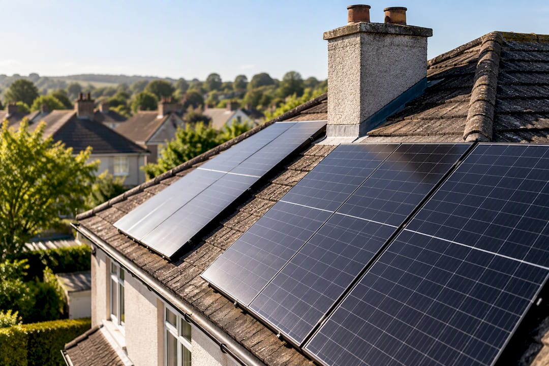
Pro Tip: Don’t just compare efficiency percentages on a spec sheet. Ask your installer for the panel’s expected annual degradation rate too. A slightly less efficient panel with a lower degradation rate can out-produce a higher-efficiency panel over 20 years.
Temperature behaviour is where n-type quietly earns its premium. Every solar panel loses some output as it heats up, but the rate of loss, the temperature coefficient, varies by architecture. N-type modules typically post coefficients around −0.29% to −0.34% per °C, while PERC panels usually run steeper, at −0.35% to −0.41% per °C. On a south-facing roof that regularly hits cell temperatures well above 25°C in summer, that difference compounds daily. Readers wanting the full mechanics of how this affects string sizing and inverter choice can dig into how temperature coefficient shapes solar output.
Bifaciality is another area where the gap is wide rather than marginal. Many n-type modules, particularly HJT, are built bifacial by default, capturing reflected light on their rear surface for an additional 5 to 15% yield depending on mounting height and ground albedo. PERC bifacial options exist but are less common and generally deliver gains at the lower end of that range, closer to 0 to 10%.
Here’s how those individual gaps compound over a panel’s working life:
- A 2% absolute efficiency advantage, held consistently over 25 years, adds up to a noticeably higher total kilowatt-hour yield, not just a slightly higher headline number on day one.
- Lower annual degradation (roughly 0.25–0.4% per year for n-type versus 0.45–0.6% for PERC) means the gap between the two technologies widens every single year the system operates.
- The combined effect of a modest efficiency edge and lower degradation is why the SurgePV analysis concludes n-type modules deliver measurably higher lifetime energy yield, even accounting for the higher purchase price.
- By year 25, typical n-type warranty power retention sits around 87 to 92%, against roughly 82 to 87% for PERC, a gap that only shows up if you actually read the small print on the warranty document.
Warranty terms deserve a specific mention because they’re where marketing language and physical reality can drift apart. A 25-year warranty is meaningless on its own; what matters is the guaranteed power retention percentage at year 25, and whether that figure is backed by independent testing or simply the manufacturer’s own projection. Always ask to see the actual degradation curve, not just the headline warranty length. For a broader look at which specific branded panels currently lead on these figures, comparing TOPCon, HJT and IBC modules available for Irish homes is a useful next step once you’ve settled on an architecture.
Degradation risks and what to ask before you sign
Efficiency numbers get the headlines, but degradation risk is what actually determines whether your system meets its 25-year promise. Three failure modes matter most, and they don’t affect n-type and p-type equally.
Light-induced degradation (LID) is the p-type problem discussed earlier: boron-oxygen complexes forming under early sunlight exposure, trapping carriers and cutting output in the first weeks of operation. N-type cells, doped with phosphorus rather than boron, largely avoid this specific mechanism, which is part of why their first-year performance curve looks flatter.
Light and elevated Temperature Induced Degradation (LeTID) is a subtler, longer-developing cousin of LID that can affect both cell types, though it has historically been more associated with certain p-type multicrystalline processes. Industry degradation reporting notes that manufacturers have adjusted gallium doping levels, wafer thickness and process controls specifically to reduce LeTID exposure, which shows this isn’t a solved problem so much as a managed one.
Potential Induced Degradation (PID) is a different animal entirely, caused by voltage stress between the cell and its grounded frame rather than by the dopant itself. PID can affect any cell type if the encapsulant and cell passivation aren’t up to standard, which is why manufacturer-specific testing matters more than the n-type or p-type label alone.
Before signing an installation contract, ask your installer these questions directly:
- What PID resistance testing has the panel manufacturer published, and is it independently verified?
- What’s the measured (not projected) first-year LID figure for this specific panel model?
- Are the junction boxes and bypass diodes rated and tested for the expected operating temperature on this specific roof?
- What’s the annual degradation assumption built into the 25-year warranty, and is it stated in the contract or just marketing material?
Updated industry guidance on failure modes makes clear that reliability testing standards are still catching up with newer cell architectures. That’s not a reason to distrust n-type technology, but it is a reason to ask for evidence rather than accepting a warranty length as proof of quality on its own.
How to choose between n-type and p-type for your home
Run through this checklist before comparing quotes, since the right answer genuinely depends on your specific roof and budget, not on which technology is newer.
- Assess your available roof space. If your roof is small, shaded in places, or oddly shaped, the higher efficiency of n-type panels lets you extract more power from limited area, which can matter more than the price difference.
- Set your premium tolerance. With the n-type cost premium narrowing to roughly 5 to 10% over PERC, decide whether that upfront gap is affordable given your total system budget.
- Consider your appetite for bifacial gains. Elevated mounts, flat roofs, or reflective ground surfaces near the array make bifacial n-type panels considerably more worthwhile than on a standard pitched roof close to slate tiles.
- Match your payback horizon. If you plan to stay in the property for 20 plus years, the compounding degradation advantage of n-type has more time to pay off; shorter horizons shrink that advantage.
- Check string design and Voc limits. Ask your installer whether the panel’s open-circuit voltage and temperature coefficient are compatible with your chosen inverter or power optimiser, particularly for larger arrays split across multiple strings.
- Request architecture specifics in writing. Don’t accept “n-type” or “p-type” as a description on a quote; ask for the exact cell architecture (TOPCon, HJT, PERC or IBC) and the manufacturer’s data sheet.
A useful companion resource here is a structured checklist for comparing solar quotes, which walks through exactly what line items and warranty terms to demand before signing anything.
Beyond solar: how doping reshapes the band structure
Doping doesn’t just add spare charge carriers, it fundamentally reshapes how easily a semiconductor conducts electricity by shifting its energy band structure. Every semiconductor has a bandgap, the energy gap between its valence band, where electrons normally sit, and its conduction band, where they can move freely and carry current.
Undoped, or intrinsic, silicon has very few carriers crossing that gap at room temperature, which is why pure silicon barely conducts at all. Adding phosphorus for n-type doping introduces donor energy levels sitting just below the conduction band, so electrons need only a small energy nudge to jump across and conduct. Adding boron for p-type doping does the mirror opposite: it creates acceptor levels just above the valence band, making it easy for electrons to jump up and leave holes behind in the valence band.
This is bandgap engineering in its simplest form, and it’s the reason doped silicon conducts electricity millions of times more readily than the pure crystal. The position of the Fermi level, effectively the “average” energy state of electrons in the material, shifts towards the conduction band in n-type material and towards the valence band in p-type material. That shift is precisely what determines how a pn junction behaves once the two materials are joined, and it’s the underlying reason n-type and p-type cells generate slightly different voltage outputs even from otherwise identical silicon.
Manufacturing challenges unique to each doping process
N-type and p-type doping each bring their own production headaches, and understanding them explains part of why n-type panels still carry a price premium, however narrow it’s become.
Boron diffusion, the standard p-type process, is well understood and forgiving at scale, which is exactly why PERC production lines were cheaper to establish. Its main challenge is precisely the boron-oxygen LID effect discussed earlier, which manufacturers now manage through post-production light-soaking treatments that stabilise the cell before it ships.
Phosphorus diffusion for n-type wafers is more sensitive to process temperature and doping uniformity, since achieving the longer carrier lifetimes n-type is prized for requires tighter contamination control throughout manufacturing. TOPCon adds a further step, depositing an ultra-thin tunnel oxide layer with extreme precision; inconsistencies here directly reduce the passivation benefit that makes TOPCon worthwhile in the first place. HJT is more demanding still, requiring low-temperature deposition of amorphous silicon layers that must be handled carefully to avoid damaging the underlying crystalline wafer, which is a large part of why HJT production costs remain higher than TOPCon’s.
None of these challenges are dealbreakers. They’re the reason n-type capacity took years to scale up to match p-type, and why the price premium, while shrinking, hasn’t disappeared entirely.
Where n-type and p-type materials show up beyond your roof
Solar panels are just one application of a doping principle that underpins almost the entire electronics industry. The same n-type and p-type building blocks that generate current in a solar cell also form the transistors inside every microchip, laptop and smartphone in daily use.
Integrated circuits rely on layering n-type and p-type regions to create millions of microscopic transistors on a single silicon chip, each one acting as a tiny switch controlled by a junction identical in principle to the one inside a solar cell. CMOS technology, the dominant chip design used in modern processors, specifically pairs n-type and p-type transistors together on the same chip to minimise power consumption, which is why your phone doesn’t need a fan.
Sensors depend on the same physics too. Photodiodes and image sensors in cameras use pn junctions to convert light into electrical signals, essentially the same charge-separation process described earlier for solar cells, just tuned for signal detection rather than bulk power generation. Temperature sensors, pressure sensors and many medical diagnostic devices use doped semiconductor junctions in similarly specialised ways.
It’s worth appreciating that the phosphorus and boron sitting in your roof panels are doing exactly the same job as the doped silicon inside your router, your car’s engine control unit and the sensor in your smoke alarm. The physics doesn’t change; only the scale and the application do.
Material availability and the environmental angle
Both boron and phosphorus are abundant, widely mined elements, so raw dopant supply isn’t a meaningful constraint on either technology. The environmental and availability questions that actually matter sit elsewhere in the supply chain.
Silver paste used for electrical contacts is a genuine cost and sustainability pressure point for both n-type and p-type cells, since silver is far scarcer than silicon and its price directly affects panel cost. Some n-type architectures, particularly TOPCon, currently require more silver per cell than PERC, which is one contributor to the ongoing price premium, though manufacturers are actively developing silver-reduction techniques to close that gap.
Manufacturing energy intensity differs too. HJT’s lower-temperature production process consumes somewhat less energy per cell than the higher-temperature diffusion steps used for PERC and TOPCon, a modest but genuine environmental point in HJT’s favour. Meanwhile, gallium, increasingly used as an alternative p-type dopant to reduce LeTID, is a byproduct of aluminium and zinc refining, making its supply somewhat more concentrated geographically than boron or phosphorus.
None of these factors should be the deciding one for a homeowner choosing a panel. But they help explain why the industry-wide shift towards n-type has taken a specific, staggered path rather than happening overnight, and why price premiums, not raw material scarcity, remain the main practical barrier.
The technology shift matters more than the marketing around it
The rapid move from roughly 30% to 70% n-type wafer share in a single year isn’t a marketing story, it’s a manufacturing one. Prices fell because production scaled, not because n-type suddenly became “better” overnight; the physics were always there.
That said, p-type PERC isn’t obsolete, and treating it as a downgrade misses the point. For a homeowner with a large, unshaded roof and a tighter budget, PERC’s slightly higher degradation and lower efficiency may simply never matter in practice, because there’s enough roof space to compensate. The trade-off is real, but it’s not universal.
If there’s one thing worth taking from this comparison, it’s that the label “n-type” or “p-type” tells you less than the actual spec sheet. Ask for the numbers behind the name.
— Get Solar Panels
Get a personalised comparison before you decide
Reading about temperature coefficients and degradation curves only gets you so far. What actually matters is how n-type and p-type panels perform on your specific roof, with your specific electricity usage, and Get Solar Panels exists to answer exactly that question without any sales pressure. A solar advice service connects homeowners with vetted, SEAI-approved local installers who can quote both architectures side by side for your address.

Start with the solar panel calculator to model how the efficiency and degradation differences discussed above translate into kilowatt-hours and euros for your own home. From there, requesting a free, no-obligation solar quote puts you in direct contact with an installer who can specify exact panel models, architectures and warranty terms for your roof. The service does not sell panels or carry out installations itself; every quote and installation decision comes from the installer, who sets final pricing. It’s a free way to turn the numbers in this article into an actual decision.
FAQ
What is the difference between n-type and p-type semiconductors?
N-type semiconductors are doped with phosphorus or another pentavalent element, giving them free electrons as the majority carrier. P-type semiconductors are doped with boron or a trivalent element instead, creating holes as the majority carrier. This dopant-level difference is what drives nearly every performance gap between the two solar cell types.
What are the disadvantages of n-type solar panels?
N-type panels typically cost more to buy, with a cost premium of roughly 5 to 10% over p-type PERC panels. Some n-type architectures, particularly TOPCon, also require more silver per cell in manufacturing, which contributes to that higher price and adds a modest supply-chain pressure point.
Are n-type solar panels worth it?
For most new residential installations in 2026, yes, particularly where roof space is limited or long-term yield matters most. N-type modules typically deliver 1 to 3% higher efficiency and lower long-term degradation than p-type PERC, and that advantage usually outweighs the narrowed price premium over a 25-year system life. Budget-limited installs with generous roof space can still get good value from p-type.
How do I identify n-type versus p-type solar panels?
Check the manufacturer’s data sheet for the specific cell architecture named, TOPCon, HJT and IBC are n-type, while PERC is p-type. If the data sheet only says “monocrystalline” without naming an architecture, ask your installer directly, since that label alone doesn’t confirm which dopant type was used.
What causes light-induced degradation in solar panels?
Light-induced degradation (LID) happens when boron and oxygen impurities in p-type silicon combine under early sunlight exposure, trapping charge carriers and reducing output. N-type cells, doped with phosphorus rather than boron, largely avoid this specific mechanism, which is one reason their first-year performance curve tends to be flatter.
Recommended
Related Articles

Best Solar Setup Ireland 2026: Complete System Design Guide
The best solar setup for Ireland 2026 — panels, inverter, battery, diverter and installer — with 4 real-world configurations, prices and paybacks.
20 Solar Panels Ireland 2026: Cost, Output, Battery & Payback
What 20 solar panels cost in Ireland 2026 (€12.7-18.6k net after grant), 7,600-8,100 kWh output, roof space, battery choice and payback vs 10 or 14 panels.
Solar Panel Temperature Coefficient Ireland 2026: How Heat Affects Output
What temperature coefficient really means for Irish solar output, real cell temps by season, 2026 brand rankings, and why low-light beats heat spec in Ireland.